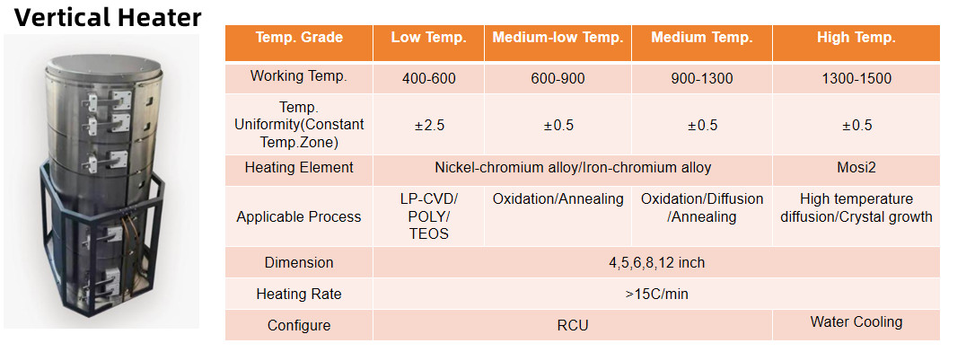
Diffusion Furnace Tube is a kind of equipment used for high temperature process, which is mainly used in the fields of semiconductor manufacturing, solar cell production and material science to achieve diffusion doping or thin film growth of impurities in materials.
Parameter Specifications:

 Detailed introduction:
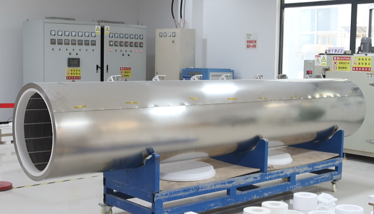
1. Basic structure: Diffusion furnace tube usually consists of the following core parts
-Furnace body: a chamber made of high temperature resistant material (e.g. stainless steel) with vacuum or controlled atmosphere maintained inside.
-Heating system: resistance wire or infrared heating element, providing uniform high temperature (800°C-1200°C).
-Quartz tubes: carrier for the silicon wafers, resistant to high temperatures and chemically inert to avoid contamination.
-Gas control system: precise passage of dopant gases (e.g. phosphane PH₃, borane B₂H₆) and inert gases (e.g. nitrogen N₃).
inert gases (e.g. nitrogen N₂).
Temperature control system: Real-time temperature monitoring and regulation with an accuracy of ±0.5°C.
-Transmission mechanism: automated wafer transmission, reducing manual intervention.
2. Working Principle: Driving the diffusion of impurity atoms into the silicon wafer through high temperature to change its electrical properties.
-Loading: Silicon wafer is put into quartz boat and pushed into quartz tube.
-Heating: Heated to a set temperature, the silicon lattice expands to accept impurities.
-Gas injection: Dopant gas decomposes and impurity atoms are adsorbed on the surface of the wafer.
-Diffusion: Diffusion of impurity atoms into the silicon interior at high temperature to form a PN junction.
-Cooling: Slowly cooling down the temperature to fix the distribution of impurities.
3.Core Applications
-Semiconductor manufacturing: doping to form the electrical structure of transistors, resistors and other components.
-Solar Cells: Preparation of P-type/N-type silicon to optimise photoelectric conversion efficiency.
-Material modification: metal heat treatment, glass coating and other processes.
4.Technical features
-Temperature uniformity: temperature difference in the furnace needs to be less than ±1°C to ensure uniform doping.
-Gas precision: flow rate control to sccm (standard millilitre/minute) level to avoid over-doping.
-Automation level: integrated PLC control, supporting process recipe storage and recall.
5.Maintenance and Challenges
-Cleaning requirements: Regular cleaning of the quartz tube to prevent deposits from affecting the temperature field.
-Safety protection: dopant gases are mostly toxic (e.g. phosphorane is flammable and explosive), requiring strict sealing and tail gas treatment.
Energy consumption control: high temperature process with high energy consumption, the new furnace tube design focuses on energy saving (e.g. multi-zone heating).
6. Comparison with ion implantation, the diffusion method is low cost, suitable for large size batch processing, but the doping depth and precision is not as good as ion implantation technology. The two are often used in combination in modern processes: diffusion for shallow junction doping, ion implantation to achieve high-precision control.
Summary: diffusion furnace tube is the basic equipment for microelectronics manufacturing, and its performance directly affects the electrical characteristics of the device. With the development of the process to the nanoscale, the equipment tends to high-precision, low-pollution and intelligent upgrade.
In the photovoltaic industry, diffusion furnace tube is mainly used to form PN junction, which is the core structure of solar cells. Emphasis needs to be placed on the use of dopant gases (e.g. phosphorus sources), the importance of temperature control, and how to optimise uniformity to improve cell efficiency. The semiconductor industry, on the other hand, is more concerned with the precision of doping, which may involve more complex structures such as shallow junction doping, as well as combinations with other techniques such as ion implantation.
Diffusion Furnace Tubes in the Photovoltaic Industry
1. Core applications
-PN junction preparation: through phosphorus (P) or boron (B) doping, the formation of P-type or N-type semiconductor layer on the surface of the wafer, constituting the core structure of the solar cell (e.g., phosphorus diffusion of P-type wafers to form the N+ layer).
-Selective emitter: optimise the doping concentration distribution, reduce the surface compound loss, and enhance the photoelectric conversion efficiency (e.g. PERC cell process).
2. Process characteristics
-Doping gas: mainly use phosphorus source (e.g. POCl₃ liquid source gasification) or boron source (e.g. BBr₃) to generate active impurity atoms through high temperature decomposition.
-Temperature range: 800°C-950°C, temperature uniformity is required within ±1°C to ensure doping uniformity for large area wafers (e.g. M10/G12 size).
-Gas control: Nitrogen (N₂) is introduced as a carrier gas and oxygen (O₂) is used to generate the phosphor-silicon glass (PSG) layer, which is subsequently removed by hydrofluoric acid (HF) etching.
-Capacity optimisation: Supports multi-slice (e.g. hundreds of slices/furnace) batch processing, with a single process time of about 1-3 hours, adapted to the needs of GW-scale PV production lines.
3. Technical Challenges
-Uniformity control: Increasing wafer size (e.g. from M2 to G12) requires optimisation of quartz boat design and airflow distribution.
-Impurity concentration gradient: through multi-step temperature control and gas flow adjustment, to achieve the doping distribution of high concentration on the surface and low concentration in the body.
-Cost control: reduce POCl₃ consumption and tail gas treatment cost (e.g. phosphoric acid recovery).
4. Industry trends
-TOPCon batteries: Higher temperature (~900°C) boron diffusion process is required, which puts higher demands on furnace tube temperature resistance and cleanliness.
-Phosphorus-free diffusion technology: development of new doping sources (e.g. ionic liquid doping) to reduce pollution.
the semiconductor industry in the diffusion furnace tube
1. Core applications
-Doping process: the formation of transistor source / drain, resistance, capacitance and other device structures (such as boron diffusion to form P traps, phosphorus diffusion to form N + contact).
-Oxidation and annealing: high-temperature oxidation to generate SiO₂ layer, or by annealing to repair lattice damage after ion implantation.
-Thin film deposition: some diffusion furnace integrated LPCVD (low pressure chemical vapour deposition) function for polysilicon, silicon nitride thin film growth.
2.Process Features
High-precision control: doping concentration accuracy up to 10¹⁵-10²⁰ atoms/cm³, temperature control within ±0.5°C. -Shallow junction doping: for polycrystalline silicon, silicon nitride thin film growth.
-Shallow junction doping: For advanced processes (e.g. below 28nm), the diffusion depth needs to be controlled to the nanometer scale, often combined with ion implantation.
-Gas system: High purity gases (e.g. B₂H₆, PH₃) are used, with toxic gas monitoring and tail gas incineration.
-Cleanliness requirements: particle contamination in the furnace tube is controlled to Class 1 level (≤1 particle per cubic foot, particle size ≥0.1μm).
3.Technical Challenges
-Thermal budget control: Avoid high temperature leading to deformation of the device structure (e.g. FinFET's fin structure).
Doping uniformity: the difference in impurity concentration between the edge and the centre area of a 12-inch wafer needs to be <2%.
-Material compatibility: Avoid reaction between quartz tubes and silicon wafers and dopant gases (e.g. metal contamination) at high temperatures.
4. Industry Trends
-3D integration: development of low temperature diffusion process (<800°C) for 3D NAND and GAA transistors.
-Advanced gas source: Adopt solid-state doping source (e.g. BN chips) instead of gas source to improve safety and controllability.
-Intelligent upgrade: Integrated AI algorithms to optimise process recipe and adjust temperature and gas flow in real time.